the beta diaries, 3rd installment
2007-10-08 by drmabuce
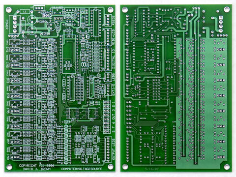
Hi All
When i deal with a large, multi-part project like this i subscribe
firmly to the policy of divide and conquer. Mr. Brown was particularly
helpful to me in this effort in describing criteria by which i could
determine that the functional sections of the CVS (Power
supply,Processor/Dacs, digital I/O and Analog Input/ADCs) were working
as i completed them. But there comes a time when one must face the
integration step; when all the dancers have to get on stage at once
and become a show. This large-scale integration includes mounting the
guts and the brain in the cabinet or panel. i am particularly rough on
a board at this stage because of my own very peculiar aesthetic (or
ANTI-aesthetic as many could effectively argue!) sensibilities. While
i respect the benefits of the functional durability of the
'basic-black,open back' panel*. it just ain't my bag. i had a
transparent box fabricated for a PSIM back in the day. i designed the
box to provide a lot of open space around the PSIM PCB but when i got
the CVS PCB i realized that -with a little creativity- and SOME
CAREFUL planning i could use it for the CVS's more than doubled
capabilities. But this meant i had to do a lot of temporary mounting
and removing and sort of sculpt the control surfaces around the PCB.
This is why i say i'm rough on PCB's. But there is a beneficial
by-product of this method. It shakes out the bugs early and i LOVE to
find the weaknesses in my workmanship in my workshop rather than at a
gig when the promoter is only giving us 20 minutes to set up!
and i found some...
 Output LED#1 never seemed to light during early tests and i mentally
  sidelined that issue to a suspicion about the LED driver circuit.
But i also noted that the 1st 4 outputs didn't seem to behave in the
same way as the last 4. After some mounting and re-mounting i was
dismayed to discover that the first four outputs just up and quit
entirely. At the risk of oversimplification, i was forced to recognize
that my first SMT soldering job , maybe, wasn't as durable as it
looked. So i got out my fine-point iron and simply re-melted each leg
of U2. and voila!  i had good stable, perfectly controllable behavior
on every output EXCEPT output 1. It was this issue that taught me the
most about soldering SMT. Output 1 comes from pin 2 of U2.  A
continuity test revealed that this pin , while feeling stationary, was
not making contact with it's pad. i made a couple of further attempts
to mate pin to pad without solder bridges but i got concerned about
heat-stressing this delicate and expensive IC. Worse, i applied too
much pressure with the very pointy tip of my iron and i nicked the PCB
trace connected to the pad.  Electrically, the pad was still connected
but decided that i was not going to trust an output to a physically
compromised connection. My solution was to VERY carefully raise pin 2
off the pad and jumper it with a very short wire directly to the base
of the LED driver transistor. That did the trick. The outputs have
been 100% ever since.
Lessons Learned:
First, i want to stress that i find NO fault in the PCB layout or
quality. In fact, the layout made my jumper kluge very easy to
implement. The nick in the pin-2 trace was squarely and unequivocally
 the result of my own fumbled attempts to force pin 2 into submission.
The root cause, i discover, is that i did not align U2 symmetrically
  on it's pads when i soldered it the first time. My mistake was that
i aligned the IC while looking at it from one side only (pins 9-16). i
was focused on getting the pins lined up, front-to-back and i laid the
chip down in a way that exposed what i saw as a good amount of exposed
pad for soldering. The problem was of course that i was giving
short-shrift to the pads on the OTHER side (pins 1-8) and on THAT side
the pins were right at the pad-edge where trace meets pad. This made
the soldering on the other side more difficult and , as i learned, not
as reliable.
The moral of this story, Line up the SMT parts while looking at ALL
the pins and balance the coverage of pin to pad EVENLY on both sides.
(remember to solder 2 corner pins to hold the alignment while you
solder the rest of them)

All in all, this is a mighty small pothole in the scale of the project
and it was , by my standards, VERY easy to diagnose and fix. i
stabilized the raised pin with a tiny dab of silicone goo, (so it
won't rattle off over time and i've been torture testing it for a
couple of days now, with admirably stable results.

Frankly, Murphy's law being the law of the land , i'd have been more
nervous if NOTHING had gone wrong! Now i feel very confident about
debugging if more is ever needed.

onward!
-doc


* i cannot mention this without a nod to it's most eloquent defender,
the late lamented John 'konkuro' Mitchell. I miss his discourse very
much.